
For a Stronger Semiconductor
IRLabs Gives High-Tech Microscope to University of Arizona Cleanroom
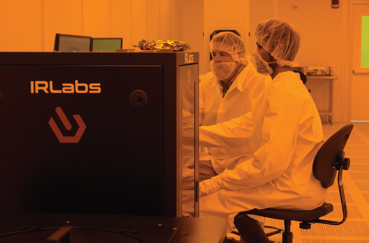
IRLabs, a Tucson-based optics and cryogenics company founded by a University of Arizona alumnus, donated a high-performance infrared emission microscope system to the UA’s Center for Semiconductor Manufacturing.
The system is installed in the ISO 5 semiconductor cleanroom, part of a recently expanded, state-of-the-art nanofabrication facility.
It helps researchers and students detect and analyze near invisible defects inside modern semiconductor devices before they lead to costly production failures. Even a single defect can result in millions of dollars in losses during semiconductor production.
IRLabs founder Frank Low, a UA scientist who died in 2009, invented infrared telescopes to observe distant galaxies and star formation. He adapted the technology in the mid-1990s for use with Intel’s computer chips. Intel and NVIDIA use this infrared emission microscope, known as IREM, during production to ensure quality.
As semiconductor devices continue to shrink, identifying failure points has become increasingly challenging. IRLabs’ IREM technology detects ultra-low levels of infrared photon emissions caused by defects such as leakage currents, hot spots and junction anomalies — without damaging the device.
It uniquely allows for inspection through silicon and packaging, preserving devices while enabling precise defect localization. This capability is important as advanced semiconductor nodes push the limits of manufacturing precision.
The donated system will allow UA students and researchers to train on the same class of tools used by leading semiconductor makers to ensure quality and reliability. It also supports Arizona’s growing role in semiconductor innovation by contributing to workforce development and research capacity.
IRLabs has a long history of innovation in infrared detection technologies, with applications in astronomy, defense and semiconductor manufacturing. The company’s continued collaboration with UA reflects a shared commitment to advancing research, education and industry impact.
“At the University of Arizona, we believe the most transformative research occurs at the intersection of world-class expertise and state-of-the-art infrastructure,” said Tomás Díaz de la Rubia, UA senior VP for research and partnerships. “Strategic partnerships like this allow us to bridge the gap between academic discovery and workforce readiness, reinforcing our role as a cornerstone of the state’s thriving semiconductor ecosystem.”
The Center for Semiconductor Manufacturing, located in the UA’s Electrical and Computer Engineering Building, was recently renovated with support from a $35.5 million award from the Arizona Commerce Authority.
It meets International Organization for Standardization 5 classification, meaning it is a highly controlled environment with stringent requirements for air cleanliness, which is crucial to protect sensitive chips from dust and particles during manufacturing.
Pictured above – The infrared microscope is widely used to identify defects and conduct failure analysis of semiconductor chips, which are the foundation of today’s advanced technology.
Photo by Kris Hanning/Office of Research and Partnerships